Emergence of Extreme Ultraviolet Lithography: Transforming the Future of Semiconductors
In recent years, a groundbreaking technology known as Extreme Ultraviolet Lithography (EUV) has been paving the way for significant advancements in semiconductor manufacturing. The emergence of EUV is not only transforming the semiconductor industry but also shaping the future of technology as a whole. This blog post delves into the journey of EUV lithography, its impact on semiconductor manufacturing, and its promising future.
Understanding EUV Lithography
What is EUV Lithography?
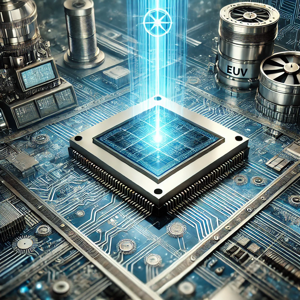
Extreme Ultraviolet Lithography is a cutting-edge technology used to create microchips with incredibly fine features. Unlike traditional lithography that uses deep ultraviolet light, EUV employs extremely short wavelengths, around 13.5 nanometers. This allows for more precise patterning, enabling the production of smaller and more efficient semiconductors.
How Does It Work?
The process of EUV lithography involves directing EUV light onto a silicon wafer to create intricate patterns. The core components of this technology include the light source, photomask, and photoresist. The light source generates the EUV light, which passes through the photomask to project a patterned image onto the wafer. The photoresist, a light-sensitive material on the wafer, captures this pattern, ultimately forming a microchip.
Evolution of EUV Lithography
The development of EUV lithography is the culmination of years of research, engineering, and collaboration among scientists and industry leaders. Initially conceptualized in the early 1990s, EUV faced numerous challenges, including the need for a reliable light source and the creation of defect-free photomasks. Over the past few decades, significant strides have been made in overcoming these hurdles, making EUV a viable technology for semiconductor manufacturing.
Challenges and Breakthroughs
One of the most notable challenges in EUV lithography was generating sufficient EUV light intensity. Traditional light sources were inadequate for producing the required wavelengths, leading to the development of plasma-based light sources. Another breakthrough came with the creation of advanced photomasks that could withstand the intense energy of EUV light without defects.
Impact on Semiconductor Manufacturing
Greater Miniaturization
EUV lithography has revolutionized semiconductor manufacturing by enabling greater miniaturization. This technology makes it possible to produce smaller and more powerful microchips, which are essential for driving advancements in various technologies, from smartphones to artificial intelligence.
Enhanced Performance and Efficiency
With EUV, manufacturers can produce semiconductors with more transistors packed into a smaller space. This not only increases the performance capabilities of devices but also enhances their energy efficiency. As a result, the next generation of electronic devices will be faster, more powerful, and more energy-efficient.
Cost-Effectiveness
Although the initial investment in EUV technology is significant, it offers long-term cost benefits. The ability to produce more semiconductors on a single wafer reduces manufacturing costs. Over time, this will lead to more affordable advanced technology for consumers.
The Future of EUV Lithography
Continuous Innovations
The journey of EUV lithography is far from over. Continuous innovations are essential for overcoming the remaining technical challenges and pushing the boundaries of what is possible. Researchers are exploring new materials and methods to enhance the efficiency and capabilities of EUV lithography further.
Global Collaboration
The advancement of EUV technology relies on global collaboration among research institutions, semiconductor manufacturers, and technology companies. This collective effort is crucial for addressing the complex challenges and ensuring the widespread adoption of EUV in semiconductor manufacturing.
Broader Applications
While EUV lithography is primarily associated with semiconductor manufacturing, its potential applications extend beyond this industry. Future developments could see EUV technology being utilized in fields such as nanotechnology, biomedicine, and materials science, opening new avenues for innovation and technological growth.
Conclusion
The emergence of Extreme Ultraviolet Lithography marks a revolutionary milestone in the semiconductor industry. By enabling the production of smaller, more efficient, and more cost-effective microchips, EUV is reshaping the technological landscape. As continuous innovations and global collaborations drive this technology forward, we can anticipate even more transformative advancements that will shape the future of various industries. Extreme Ultraviolet Lithography is not merely a technological breakthrough; it is the gateway to the next era of technological innovation.